Heterogenous integration (HI) technologies, including advanced packaging, will be critical to achieving the performance, power, area, and cost demands of future microelectronic products. While HI is based on the technologies for inter- chiplet interconnects and chiplet assembly, currently, technologies have been developed mostly for high bandwidth memory (HBM) and chiplets integrated on interposers/PCB with relatively low inter-chiplet interconnect density at a high cost. These technologies include those for HI building blocks, such as through-silicon-via (TSV), microbump (μbump), copper direct bonding, silicon (or glass) interposers, RDL/substrates, and die-to-die or die-to-wafer 2.xD assembly. For future systems of ever higher performance, power, and functionality, HI fabrication must address the grand challenges such as High interconnect density at low cost, and High interconnect power efficiency. This research topic will focus on the interconnect pitch scaling for 3D HI building blocks to enable very high inter-chiplet interconnect density at low cost using technologies such as nano-TSVs, fine-pitch low-temperature hybrid bonding, and fast assembly with nanoscale resolution.

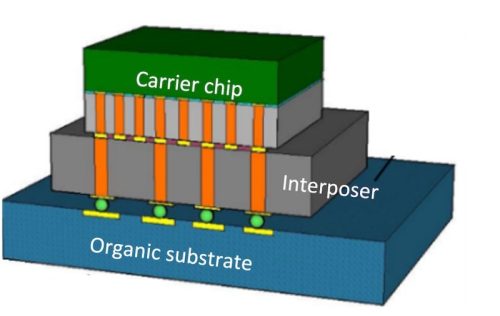
2.5D/3D system integration with fine-pitch interconnects