“Heterogeneous 3D integration” enables each thin device layer to be fabricated separately and then stacked vertically with each other using through-silicon vias. However, the current “Heterogeneous 3D integration” with microscale through-silicon vias with a diameter ranging from 1µm to 5µm could not meet the future interconnection densities requirement. The through-silicon vias (TSV) diameter has to be pushed from the microscale to the nanoscale which is below 100 nm at aggressive technology nodes. From the fabrication aspects, nanoscale via etching, metallization, and via filling, as well as the via alignment and bonding at the nanoscale are all very challenging. In this research area, we will demonstrate, test, and investigate the nanoscale via reliability in terms of thermal behaviors, thermal-mechanical stresses, and electrical behaviors using dedicated test vehicles and finite element simulations (FEM).

TSV fabrication process flow and demonstrations
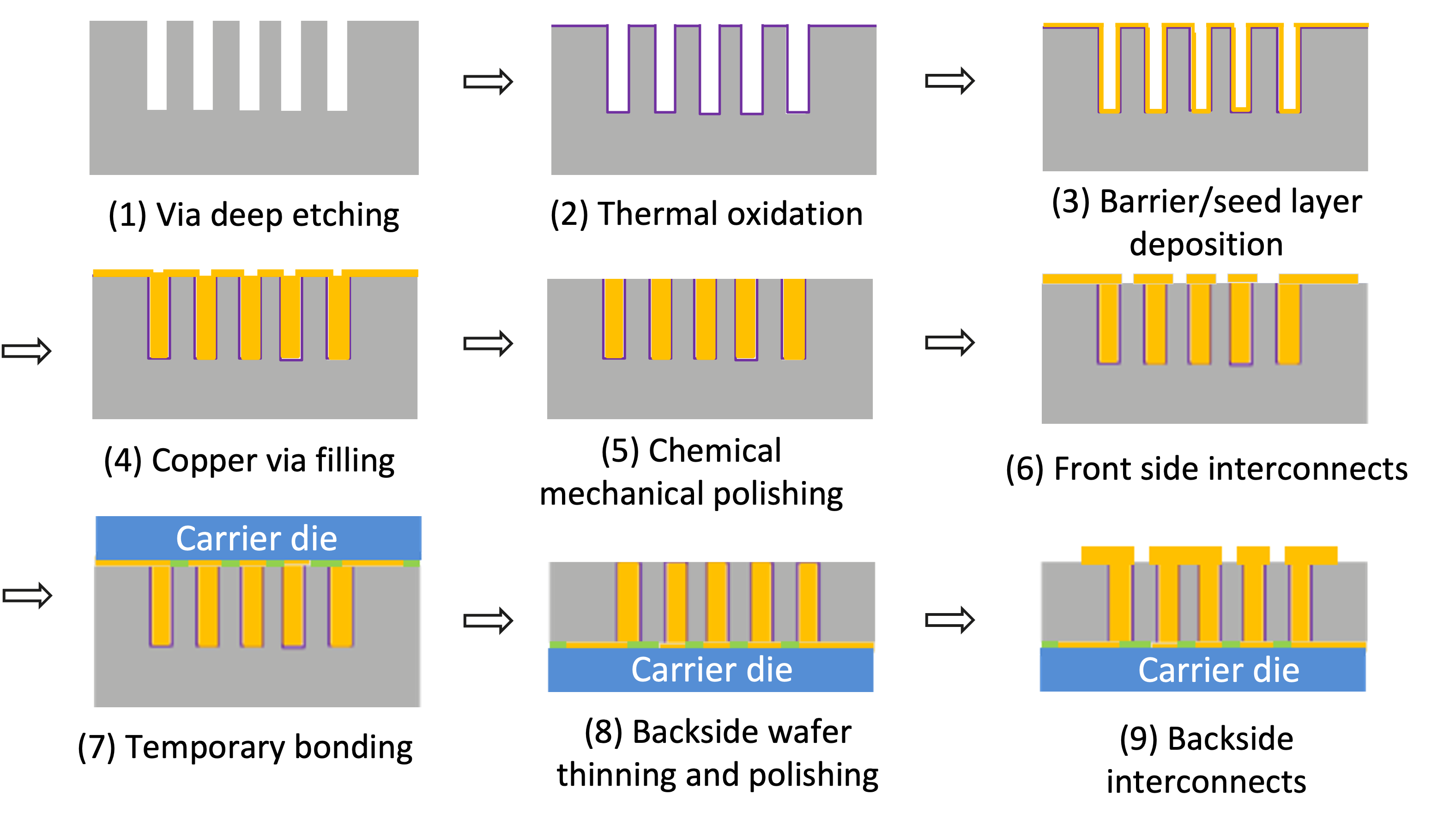
Figure 1 illustrates the standard TSV fabrication process, including deep via etching, via dielectric insulation, and via filling. The critical processes are step (c) deposition of barrier, adhesion liner, and seed layers along the TSV for preventing metal diffusion, enhancing metal adhesion strength, and facilitating the metal electroplating process, respectively. Step (d) is the critical TSV fill step accomplished by chemical vapor deposition (CVD) or electroplating.