
With the rapid development of microelectronics, the pursuit of better performance and smaller system size inevitably leads to higher power density, rendering an extremely large heat flux on a small area. Many advanced cooling technologies, such as impingement jet cooling and microchannel cooling, have been proven effective in dealing with heat dissipation issues in electronics. The optimal design and fundamental understandings of these techniques are urgently needed to improve the heat transfer efficiency in various application scenarios.
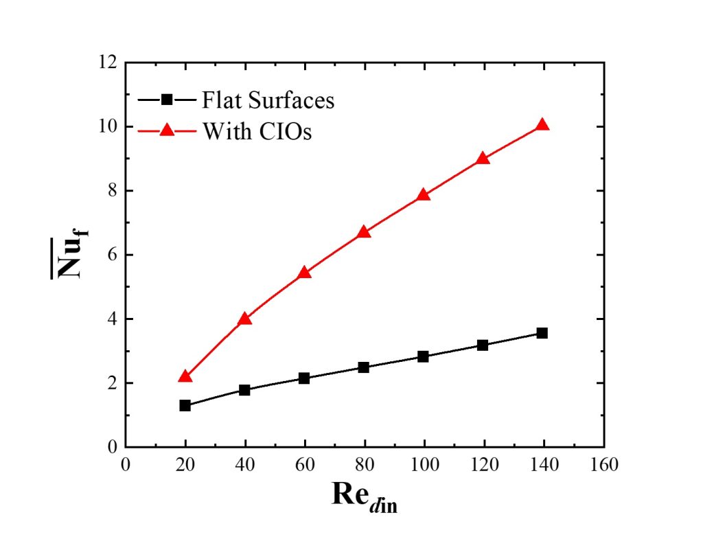
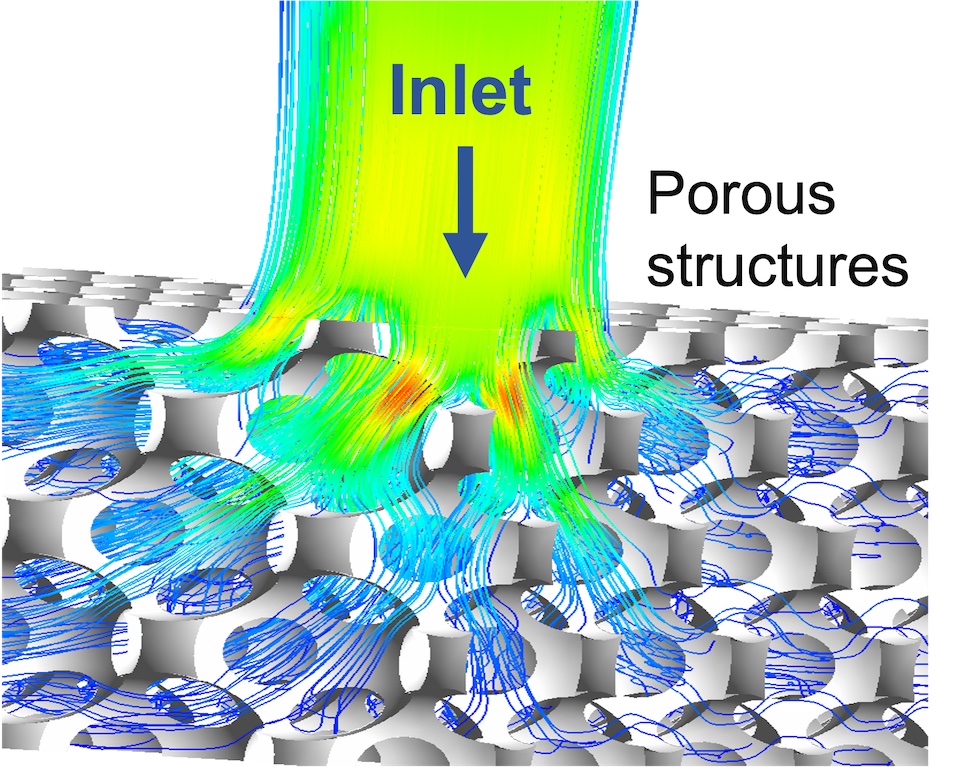
Copper inverse opals (CIOs) are porous structures deposited on around a matrix of sacrificial microspheres with regular arrangements on a silicon substrate with a thin Au metal layer. CIOs have attracted extensive research interest due to their great potential in enhancing heat transfer especially in boiling heat transfer by providing high-density nucleation sites. The excellent thermal conductivity of copper ensures good thermal conduction in solid materials. And also, a large number of interconnected pores in CIOs allows fluids to transport between the solid porous structures and thus significantly enhances the convective heat transfer. Therefore, the superior heat transfer characteristics make CIOs promising materials for single-phase impingement jet cooling. However, further studies are still needed to couple CIOs in the design of advanced jet cooling technologies to achieve optimal heat dissipation.
In this project, we target to understand the thermofluidic properties of CIOs in a single-phase cooling system and help to build a guideline for the design of cooling systems with CIOs. The heat transfer and flow characteristics of the system are modeled and benchmarked at different design factors, e.g., inlet velocity and nozzle-to-CIO height.
Summary:
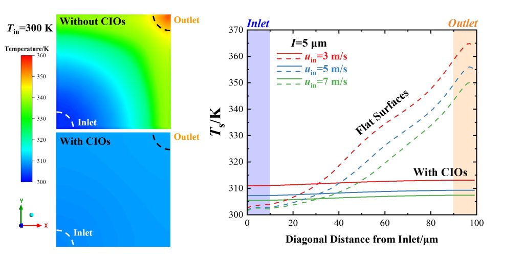
- Utilization of CIOs in single-phase jet coolers enables a lower and more uniform temperature on the chip interface.
- However, large flow resistance in CIOs will increase the total pressure drop of jet cooler.
- Increasing the nozzle-to-CIO distance results in a stronger bypass flow and thus decreases the pressure drop and Nusselt number.
- A reduced-order model is proposed to describe the flow and heat transfer characteristics of jet coolers with CIOs, showing a good accuracy.