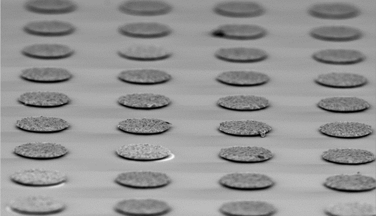
To meet the future ultra-fine pitch, high-accuracy integration, and high-density interconnections, hybrid bonding has great potential to push the bonding pitch to submicron. Hybrid bonding entails the formation of bonded regions through dielectric-dielectric interactions and electrical contacts with Cu-Cu bonding, as well as Cu-dielectric (i.e. SiO2, SiCN) interactions as Cu bonding pads on top and bottom chips are usually not the same size and/or may not be perfectly aligned. For the standard hybrid bonding process flow, the Cu metal pad is electroplated inside the defined SiO2 pattern. After the Cu pad electroplating with an over-plated copper surface, surface planarization of Cu/SiO2 using CMP processes is implemented to create an ultra-clean and small rough surface for the bonding. The hybrid bonding utilizes oxide-to-oxide bonding at room temperature and under a low bonding pressure, followed by a Cu-Cu diffusion bonding at a certain anneal temperature (200-400 °C). In this research area, we will address the following three major challenges for the metal pad pitch scaling of hybrid bonding: (1) Cu pad dishing or protrusion for submicron metal pad pitch will be more pronounced since the bump metal density increases. The CMP process optimization will be very critical and challenging; (2) The thermal expansion of the Cu-pad size will be very small as the bump pad scales to the submicron range. This will lead to different anneal temperatures and times to control the expansion of the Cu pad. (3) It will be very challenging to achieve high bonding accuracy and small misalignment for submicron bonding pad pitch, due to the limits of the hybrid bonding tools. Therefore, an innovative alignment method is needed to tackle this challenge.

Electroplating\Stencil Printing\Au Stud\Polymer Bump
