Our lab has 4 SCALE SURF positions for this summer, with topics of advanced packaging and heterogeneous integration.
Those projects are from SCALE SURF research projects. SCALE projects are restricted to students who are U.S. Citizens. By applying to this project, you can be considered for any of the SCALE projects with one application. See https://lnkd.in/gfMaX6cT to view all of the SCALE SURF research projects for summer 2023.
Nano Hub postings: https://nanohub.org/groups/scale/research_su23
Project Descriptions: https://lnkd.in/g7Es9uJm
Application: https://lnkd.in/g6Sn6EwW
SCALE Heterogeneous Integration/ Advanced Packaging: 3D Cryogenic Packaging for Superconducting Computing
Professor:
- Electrical Engineering
- Materials Engineering
- Mechanical Engineering
This project is one of several SCALE SURF research projects. SCALE projects are restricted to students who are U.S. Citizens. By applying to this project, you can be considered for any of the SCALE projects with one application. See https://nanohub.org/groups/scale/research_su23 to view all of the SCALE SURF research projects for summer 2023.
In 2017, a large-scale, 3D integrated quantum processor was demonstrated by MIT Lincoln Laboratory using heterogeneous 3D integration to create an architecture that enables the use of the third dimension without sacrificing qubit performance [D. Rosenberg, et al., Nature 2017]. In these quantum applications, conventional Sn-based solder bumps are not reliable while Indium and bismuth-based solders are promising for 3D integration at low temperatures. In this topic, new cryogenic compatible packaging materials and cryogenic superconducting multi-chip bonding techniques are needed to further explore and investigate the microelectronics devices and packages at low/cryogenic temperatures.
 Source: Alfaro-Barrantes, J. A., et al. “Superconducting high-aspect ratio through-silicon vias with DC-sputtered Al for quantum 3D integration.” IEEE Electron Device Letters 41.7 (2020): 1114-1117.
Reference: Rosenberg, D., et al. “3D integrated superconducting qubits.” npj quantum information 3.1 (2017): 1-5.)
In your application, please specify which of the SCALE technical areas you are most interested in. The technical areas are:
• Radiation Hardening
• System-on-Chip
• Heterogenous Integration/ Advanced Packaging
• Program Evaluation
Be sure to name any specific SCALE projects you are interested in, and include information about how you meet the required and desired experience and skills for each of these projects.
For US citizen students who are interested: you can become part of the Purdue microelectronics program called SCALE, sponsored by the Department of Defense. In SCALE, you will have opportunities for continuing research (paid or for credit) and industry and government internships throughout your time at Purdue. Please apply to SCALE here: https://research.purdue.edu/scale/.
More information: https://s-pack.org/
SCALE Heterogeneous Integration/ Advanced Packaging: Chip Package Interactions Metrology Development for Advanced Technology Node
- Mechanical Engineering
- Electrical Engineering
- Materials Engineering
This project is one of several SCALE SURF research projects. SCALE projects are restricted to students who are U.S. Citizens. By applying to this project, you can be considered for any of the SCALE projects with one application. See https://nanohub.org/groups/scale/research_su23 to view all of the SCALE SURF research projects for summer 2023.
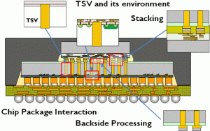
Thermo-mechanical stress of the package can be directly transferred to the semiconductor device, inducing large local stresses to drive interfacial crack formation and propagation. Therefore, the interactions between the semiconductor package stresses and the semiconductor device referred to as “Chip package interaction (CPI)” is very crucial to understand the device’s electrical behaviors under different thermo-mechanical stress levels.
For the future advanced transistors inside the dense 3D integration system with fine-grained connectivity of nanoscale vias, mechanical stress induced by the multilayer stack is expected to have a big impact on the electrical performance of the novel devices and interconnects, nano-TSVs and sensors. This research task will focus on the thermomechanical modeling and thermal stress characterizations of advanced devices and packages. Novel thermo-mechanical stress metrology will be developed using semiconductor manufacturing, Micro-electromechanical systems (MEMS) and advanced packaging techniques.
 Source: Guo, Wei, et al. “3D chip package interaction thermo-mechanical challenges: Proximity effects of Through Silicon vias and μ-bumps.” 2012 IEEE International Conference on IC Design & Technology. IEEE, 2012.
In your application, please specify which of the SCALE technical areas you are most interested in. The technical areas are:
• Radiation Hardening
• System-on-Chip
• Heterogenous Integration/ Advanced Packaging
• Program Evaluation
Be sure to name any specific SCALE projects you are interested in, and include information about how you meet the required and desired experience and skills for each of these projects.
For US citizen students who are interested: you can become part of the Purdue microelectronics program called SCALE, sponsored by the Department of Defense. In SCALE, you will have opportunities for continuing research (paid or for credit) and industry and government internships throughout your time at Purdue. Please apply to SCALE here: https://research.purdue.edu/scale/.
More information: https://s-pack.org/
SCALE Heterogeneous Integration/ Advanced Packaging: Glass Interposer Development for 3D Heterogenous Integration
- Electrical Engineering
- Mechanical Engineering
- Materials Engineering
This project is one of several SCALE SURF research projects. SCALE projects are restricted to students who are U.S. Citizens. By applying to this project, you can be considered for any of the SCALE projects with one application. See https://nanohub.org/groups/scale/research_su23 to view all of the SCALE SURF research projects for summer 2023.
Interposer is one of the most potential solutions for future 3D integration with ultrafine pitch. Silicon interposer has been developed in both industry and academia. However, silicon interposer has limitations, such as low productivity due to limited wafer size, extra expensive semiconductor fabrication processes, and poor electrical properties like insert loss and signal crosstalk. On the contrary, glass can be one kind of promising material as an interposer because of its excellent properties, such as good electrical resistivity, relatively low CTE compared to organic material, and possible high productivity with big panel sizes provided by glass suppliers.
Recent research studies have mainly focused on three challenges in glass interposer technology: (1) formation of the fine pitch via, which is more difficult than through silicon via (TSV) due to the unfavorable etching process ; (2) via metallization and via filling process, which become much more complicated because of the rough morphology of TGV surface, and difficulty to fill the tapered via through Damascus electroplating; (3) reliability concern, which is caused by brittleness and poor mechanical strength of glass.

Through glass via fabrications
Reference: Wei, T. W., Cai J.*, et al. Performance and reliability study of TGV interposer in 3D integration[C]//2014 IEEE 16th Electronics Packaging Technology Conference (EPTC). IEEE, 2014: pp. 601-605.
In your application, please specify which of the SCALE technical areas you are most interested in. The technical areas are:
• Radiation Hardening
• System-on-Chip
• Heterogenous Integration/ Advanced Packaging
• Program Evaluation
Be sure to name any specific SCALE projects you are interested in, and include information about how you meet the required and desired experience and skills for each of these projects.
For US citizen students who are interested: you can become part of the Purdue microelectronics program called SCALE, sponsored by the Department of Defense. In SCALE, you will have opportunities for continuing research (paid or for credit) and industry and government internships throughout your time at Purdue. Please apply to SCALE here: https://research.purdue.edu/scale/.
More information: https://s-pack.org/
SCALE Heterogeneous Integration/ Advanced Packaging: Self-alignment Technology for 3D System Integration
- Electrical Engineering
- Mechanical Engineering
- Materials Engineering
This project is one of several SCALE SURF research projects. SCALE projects are restricted to students who are U.S. Citizens. By applying to this project, you can be considered for any of the SCALE projects with one application. See https://nanohub.org/groups/scale/research_su23 to view all of the SCALE SURF research projects for summer 2023.
For the typical 3D integration scheme, die-to-wafer bonding is a key technology that can enable the stacking of different chips, such as logic, memory, or power devices. Compared with wafer-to-wafer bonding, it is challenging for die-to-wafer bonding to achieve high throughput while maintaining a high alignment accuracy. Researchers have been investigating different self-alignment technologies to improve the high-precision chip alignment accuracy for die-to-wafer bonding, such as Surface tension-driven with hydrophilic chip surfaces. In this topic, we will explore innovative self-alignment methods for advanced die-to-wafer bonding, enabling high throughput heterogeneous integration.

Reference: Fukushima, Takafumi, et al. “Self-assembly technologies with high-precision chip alignment and fine-pitch microbump bonding for advanced die-to-wafer 3D integration.” 2011 IEEE 61st Electronic Components and Technology Conference (ECTC). IEEE, 2011.)
In your application, please specify which of the SCALE technical areas you are most interested in. The technical areas are:
• Radiation Hardening
• System-on-Chip
• Heterogenous Integration/ Advanced Packaging
• Program Evaluation
Be sure to name any specific SCALE projects you are interested in, and include information about how you meet the required and desired experience and skills for each of these projects.
For US citizen students who are interested: you can become part of the Purdue microelectronics program called SCALE, sponsored by the Department of Defense. In SCALE, you will have opportunities for continuing research (paid or for credit) and industry and government internships throughout your time at Purdue. Please apply to SCALE here: https://research.purdue.edu/scale/.
More information: https://s-pack.org/