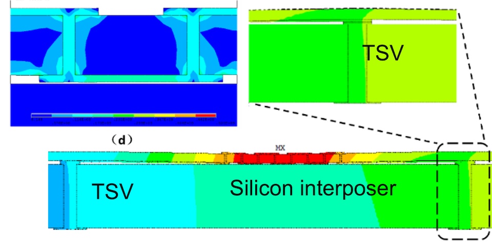
Thermo-mechanical stress of the package can be directly transferred to the semiconductor device, inducing large local stresses to drive interfacial crack formation and propagation. Therefore, the interactions between the semiconductor package stresses and the semiconductor device referred to as “Chip package interaction (CPI)” is very crucial to understand the device’s electrical behaviors under different thermo-mechanical stress levels.
For the future advanced transistors inside the dense 3D integration system with fine-grained connectivity of nanoscale vias, mechanical stress induced by the multilayer stack is expected to have a big impact on the electrical performance of the novel devices and interconnects, nano-TSVs and sensors. In our research plan, we will focus on the thermomechanical modeling and thermal stress characterizations of advanced devices and packages. Novel thermo-mechanical stress metrology will be developed using semiconductor manufacturing, Micro-electromechanical systems (MEMS), and advanced packaging techniques.
